
Plasma 切割方案
内容介绍
传统锯片或激光切割的可行替代方案 – 正在进入第三代半导体SiC领域
并行处理:“高芯片密度下极高”的切割效率和效益
最小的切割道:提升单晶圆上的芯片产量(最多增加80%)
极高的性能上限:超薄晶圆(30um)、边缘处理和低损伤
高度配合晶圆设备,提供更大的工艺灵活性, 晶圆级先进封装
The most popular trend and solutions for the new type of books used in everything:
1. Trends and causes
1. The changing process of crystal daily degree:
1. A conventional 12-inch star-shaped sunglass is about 280 microns to 400 microns after full thinning.
2. Ultra-thin wafers - below 100um: Conventional wafers used for stacked packaging are below 100 microns, while more advanced packaging requires 50 microns.
3. Latest: Currently, the thinnest wafer has developed to a thickness of 30 microns, which meets the needs of multi-layer difficult packaging such as 25D-3DIC and advanced storage.
2. Reasons for super reliance on crystal:
1. The core is to meet the requirements of advanced packaging, complex packaging, but not too much sacrifice in the size of the xy and z axes. Therefore, when the size is very important, the diversified packaging technologies (PIP (package in package), POP (packaging on package), multi-chip, system-level packaging and 2.5-3D packaging, etc.) all require the circumference of the star to be as thin as possible, leaving more space for the packaging process .
2. Thinning reduces the stress inside the chip and greatly reduces the possibility of chip breakage due to internal force, making post-packaging processing easier. Especially when it comes to heterogeneous and heterogeneous integration, the stress difference and lattice mismatch of different chips lead to shear force, which causes chip breakage, which is the most difficult problem to solve.
3. Improvement of electrical performance: Reduce the package volume while improving circuit performance, reduce high-frequency effects and time delays
4. Increase heat dissipation. The thinner the substrate is, the easier it is to conduct heat away. Especially when the chip structure is more complex and the integration is higher, the heat will gather quickly and not be easily evacuated.
2. Problems after weight loss
1. Changes in physical properties:
Excessive reduction of the product will lead to a decrease in physical rigidity, which will cause great deformation and curling under the action of gravity, and will vibrate in the moving airflow; the physical collision part of the edge is easily damaged, has sharp edges, and will adhere to other planes and be difficult to separate.
2. The difficulty of post-processing and handling will be great, and the requirements for transmission and tools will be higher:

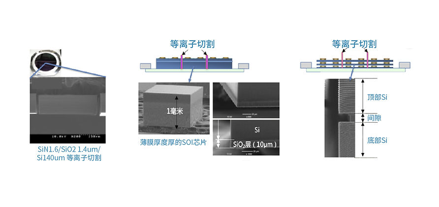
1. The edge damage is the smallest among all cutting solutions, and is most suitable for scenes that are highly sensitive to damage.
Reactive ion etching, which combines physical and chemical changes, is the best method for edge processing. There will be no burrs at the micron level, and the possible damage to the chip is minimal.
Advanced process chips use a lot of copper (Cu) or low dielectric constant materials (Low-k). Therefore, preventing burrs is more important. In the future, in 2.5D-3D packaging, especially CHIPLET in technological development, this will be a more competitive solution.
2. Ultra-thin wafers below 50 microns, down to 30 microns
Plasma cutting is required, while laser solutions may not be able to penetrate this area (50-100um thickness is more suitable), and it may not work well below that, and the impact of oblique cracks may be greater.
3. Dicing street: Dicing street has the smallest limit value
The theoretical limit of the cutting path formed by plasma cutting is the smallest, and it can easily reach the sub-micron level, which can greatly reduce the cutting loss. However, it depends on the specific materials and requirements. According to calculations, 20% more chips can be produced. Cost savings
4. In terms of speed, single crystal parallel processing can achieve extremely high speed
The cutting is completed in one go, and the efficiency is high. However, the thickness of the chip should be considered. If it is thick, it will be very difficult to cut, and the time will not be too fast. Considering thick chips is not a major application direction.
5. Can deeply collaborate with wafer process equipment
The patterning scheme of photolithography + etching is becoming more and more common. Plasma cutting has a very good equipment platform, without the need to add SD laser cutting equipment and splitting machines separately. In addition, the cost of advanced packaging is getting higher and higher, and the higher the stacking requirements, the deeper the synergy between manufacturing and packaging, making the refined processing of the front-end process before packaging more meaningful.
